- 您现在的位置:买卖IC网 > Sheet目录313 > AT45DB161B-TI (Atmel)IC FLASH 16MBIT 20MHZ 28TSOP
Features
?
?
?
?
?
?
Single 2.5V - 3.6V or 2.7V - 3.6V Supply
Serial Peripheral Interface (SPI) Compatible
20 MHz Max Clock Frequency
Page Program Operation
– Single Cycle Reprogram (Erase and Program)
– 4096 Pages (528 Bytes/Page) Main Memory
Supports Page and Block Erase Operations
Two 528-byte SRAM Data Buffers – Allows Receiving of Data
?
?
?
?
?
?
?
while Reprogramming of Nonvolatile Memory
Continuous Read Capability through Entire Array
– Ideal for Code Shadowing Applications
Low Power Dissipation
– 4 mA Active Read Current Typical
– 2 μA CMOS Standby Current Typical
Hardware Data Protection Feature
100% Compatible to AT45DB161
5.0V-tolerant Inputs: SI, SCK, CS, RESET and WP Pins
Commercial and Industrial Temperature Ranges
Green (Pb/Halide-free) Packaging Options
16-megabit
2.5-volt Only or
2.7-volt Only
DataFlash ?
Description
The AT45DB161B is a 2.5-volt or 2.7-volt only, serial interface Flash memory ideally
suited for a wide variety of digital voice-, image-, program code- and data-storage
AT45DB161B
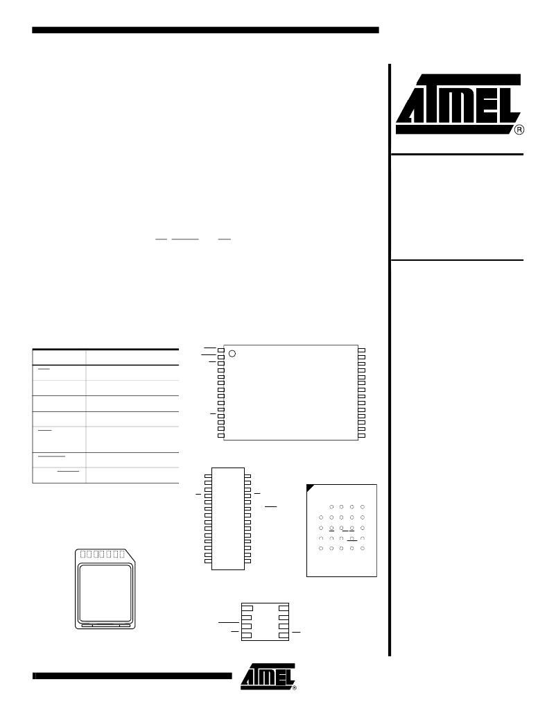
Pin Configurations
TSOP Top View – Type 1
RDY/BUSY
1
28
NC
Pin Name
CS
SCK
SI
SO
WP
Function
Chip Select
Serial Clock
Serial Input
Serial Output
Hardware Page Write
RESET
WP
NC
NC
VCC
GND
NC
NC
NC
CS
SCK
SI
SO
2
3
4
5
6
7
8
9
10
11
12
13
14
27
26
25
24
23
22
21
20
19
18
17
16
15
NC
NC
NC
NC
NC
NC
NC
NC
NC
NC
NC
NC
NC
Protect Pin
RESET
Chip Reset
SOIC
CBGA Top View
RDY/BUSY
Ready/Busy
GND
NC
1
2
28
27
VCC
NC
through Package
1 2 3 4 5
NC
CS
SCK
3
4
5
26
25
24
NC
WP
RESET
SI
SO
6
7
23
22
RDY/BUSY
NC
A
B
NC
NC
NC
NC
DataFlash Card
(1)
NC
NC
8
9
21
20
NC
NC
C
NC
SCK GND VCC
NC
Top View through Package
NC
NC
10
11
19
18
NC
NC
D
NC
NC
CS RDY/BSY WP NC
SO SI RESET NC
NC
12
17
NC
E
NC
13
16
NC
NC
NC
NC
NC
NC
7 6 5 4 3 2 1
NC
14
15
NC
CASON – Top View through Package
SI
SCK
RESET
1
2
3
8
7
6
SO
GND
VCC
Note:
1. See AT45DCB002 Datasheet.
CS
4
5
WP
Rev. 2224I–DFLSH–10/04
1
发布紧急采购,3分钟左右您将得到回复。
相关PDF资料
AT45DB321-TC
IC FLASH 32MBIT 13MHZ 32TSOP
AT45DB321B-TI
IC FLASH 32MBIT 20MHZ 32TSOP
AT45DB321C-TC
IC FLASH 32MBIT 40MHZ 28TSOP
AT45DB642-TC
IC FLASH 64MBIT 20MHZ 40TSOP
AT88CK9000-8TH
CRYPTO PROGRAMMER BOARD 8-TSSOP
AT88SC12816C-MJ
IC EEPROM 128KBIT 1.5MHZ M2J
AT88SC25616C-MJ
IC EEPROM 256BIT 1.5MHZ M2J
AT88SC3216C-MJ
IC EEPROM 32KBIT 1.5MHZ M2J
相关代理商/技术参数
AT45DB161B-TI-2.5
功能描述:IC FLASH 16MBIT 20MHZ 28TSOP RoHS:否 类别:集成电路 (IC) >> 存储器 系列:- 标准包装:378 系列:- 格式 - 存储器:闪存 存储器类型:FLASH 存储容量:8M(1M x 8,512K x 16) 速度:110ns 接口:并联 电源电压:2.7 V ~ 3.6 V 工作温度:-40°C ~ 85°C 封装/外壳:48-CBGA 供应商设备封装:48-CBGA(7x7) 包装:托盘
AT45DB161BTI25
制造商:ATMEL 功能描述:Factory programmed New parts
AT45DB161B-TU
制造商:Adesto Technologies Corporation 功能描述:28-TSOP, IND TEMP, 2.7V - Bulk
AT45DB161-CC
制造商:ATMEL 制造商全称:ATMEL Corporation 功能描述:16-Megabit 2.7-volt Only Serial DataFlash
AT45DB161-CI
功能描述:IC FLASH 16MBIT 20MHZ 24CBGA RoHS:否 类别:集成电路 (IC) >> 存储器 系列:- 标准包装:378 系列:- 格式 - 存储器:闪存 存储器类型:FLASH 存储容量:8M(1M x 8,512K x 16) 速度:110ns 接口:并联 电源电压:2.7 V ~ 3.6 V 工作温度:-40°C ~ 85°C 封装/外壳:48-CBGA 供应商设备封装:48-CBGA(7x7) 包装:托盘
AT45DB161-CNC
功能描述:闪存 16M bit
RoHS:否 制造商:ON Semiconductor 数据总线宽度:1 bit 存储类型:Flash 存储容量:2 MB 结构:256 K x 8 定时类型: 接口类型:SPI 访问时间: 电源电压-最大:3.6 V 电源电压-最小:2.3 V 最大工作电流:15 mA 工作温度:- 40 C to + 85 C 安装风格:SMD/SMT 封装 / 箱体: 封装:Reel
AT45DB161-CNI
功能描述:闪存 16M bit
RoHS:否 制造商:ON Semiconductor 数据总线宽度:1 bit 存储类型:Flash 存储容量:2 MB 结构:256 K x 8 定时类型: 接口类型:SPI 访问时间: 电源电压-最大:3.6 V 电源电压-最小:2.3 V 最大工作电流:15 mA 工作温度:- 40 C to + 85 C 安装风格:SMD/SMT 封装 / 箱体: 封装:Reel
AT45DB161D
制造商:ATMEL 制造商全称:ATMEL Corporation 功能描述:16-megabit 2.5-volt or 2.7-volt DataFlash
